Science
India Pushes Semiconductor Design Amid Global Chip Shortage
In a significant move to bolster its semiconductor industry, India is ramping up efforts to become a global hub for electronics manufacturing and design. The initiative, backed by the India Semiconductor Mission, includes a substantial outlay of ₹76,000 crore aimed at addressing the increasing global demand for semiconductors. This shift comes as the world faces a projected shortfall of 1 million chip designers by 2030, according to a report by Deloitte.
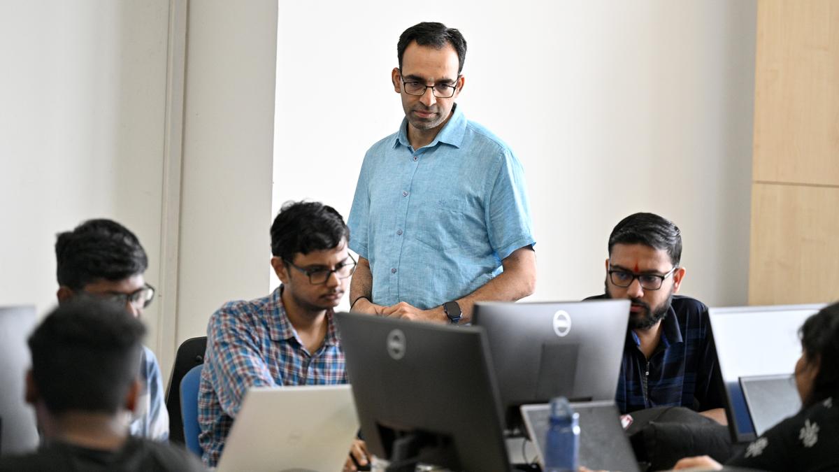
The roots of this initiative can be traced back to 2002 when Yuan Taur, a renowned professor at the University of California, San Diego, encouraged a promising student, Anuj Grover, to pursue a PhD in device design. Grover, now a faculty member at the Indraprastha Institute of Information Technology (IIIT) in Delhi, reflects on the opportunity he declined due to limited job prospects in India at the time. Today, he recognizes the transformation within the semiconductor sector, attributing it to government support and the burgeoning talent pool in the country.
Over the past two years, India has approved the establishment of ten large semiconductor manufacturing and assembly facilities across six states, including Gujarat, Punjab, and Uttar Pradesh. This infrastructure aims to capitalize on India’s significant pool of chip designers, estimated to comprise one-fifth of the global total. The country saw 5.7 lakh enrolments in electronics engineering graduate programs in the 2021-22 academic year, showcasing a growing interest in this field.
Despite these advancements, challenges persist. Critics of the government’s strategy, such as former Reserve Bank of India governor Raghuram Rajan, caution against over-reliance on subsidies for manufacturing. Rajan and his collaborator, Rohit Lamba, argue that should these incentives wane, companies may withdraw to more favorable markets. The government, however, highlights the geopolitical significance of enhancing local chip production capabilities, especially after the global supply chain disruptions witnessed during the COVID-19 pandemic.
One area of consensus between government officials and critics is the importance of intellectual property and design. India already excels in these domains and does not require extensive subsidies to advance. Unlike fabrication, which is resource-intensive and costly, chip design can be achieved with minimal equipment. Grover likens the semiconductor design process to urban planning, emphasizing the need for various roles—from architects to engineers—to collaborate effectively.
The sophistication of semiconductor technology presents additional hurdles. Chip design involves intricate layers of circuits, with billions of transistors crammed into tiny units. This complexity demands precision and reliability in production, where even minor impurities can compromise output.
To enhance accessibility to essential design tools, the Indian government has launched the Chips to Startups (C2S) program, acquiring licenses for leading electronic design automation (EDA) software at no cost to educational institutions. This initiative allows students to utilize industry-standard tools, significantly reducing previous costs that reached ₹3–4 lakh annually for individual licenses. As a result, students are now engaging in practical design projects, such as developing a 180 nanometer chip, advancing their skills from theoretical understanding to real-world applications.
Meanwhile, companies like Tessolve, a semiconductor design firm based in Bengaluru, are making strides despite the challenges. Since its establishment in 2004, Tessolve has expanded its operations across multiple countries and raised $130 million in funding this year. CEO Srini Chinamilli highlights the appeal of remote work, allowing the firm to tap into talent in smaller cities, further diversifying its workforce.
Despite government support and a promising design landscape, the gap between Indian semiconductor education and that of the U.S. remains a point of concern. The industry invests only 0.4% of its profits into academic research and development, significantly lower than the 10-15% typical in countries like the U.S. and South Korea. This disparity limits the practical training opportunities for students and hinders collaboration between academia and industry.
Grover emphasizes the need for universities to align their training programs with industry requirements, ensuring that graduates are equipped to tackle real-world challenges. He points to successful collaborations in the U.S. where academia and industry work together to solve pressing problems, benefiting both students and companies alike.
While the semiconductor chips themselves constitute only 31% of the total cost of devices like smartphones, the real value lies in design and intellectual property. To maximize the benefits from this sector, Grover argues that India must evolve into a “product nation” that creates globally desirable products. The emphasis on design is crucial, as even the seemingly simple aspects of a product, such as button placement, can be patented and form a significant portion of value.
Despite the hurdles, the hiring landscape remains robust, with companies actively seeking talent in semiconductor design. Recent reports indicate that over 60 students from BITS Pilani were recruited by NVIDIA, which is notable given the broader tech industry slowdown. Grover concludes that while challenges exist, the necessary resources and talent are readily available. The future of India’s semiconductor industry hinges on a collective will to innovate and elevate its standing in the global market.

India Seizes Opportunity to Redefine Global Economic Landscape
Major 4,670 BTC Transfer to Kraken Signals Market Movements

Arknights: Endfield Unveils Chen Qianyu in Thrilling Story Trailer

Surgeons Remove 15 kg Tumors from Woman in Complex Surgery

Zelensky Urges Inclusion of Europe in Peace Talks with Russia

Bill Bryson’s Masterful Science Writing Captivates Readers

WWE Uncovers Footage of Mystery Attacker from Survivor Series

New Challenges Await the Norris Family in Landman Season 2 Episode 4

Indian Actresses Choose Intimate Weddings Over Lavish Celebrations

SBI Announces QIP Floor Price at ₹811.05 Per Share

Cept Unveils ₹3.1 Crore Urban Mobility Plan for Sustainable Growth

New Blood Group Discovered in South Indian Woman at Rotary Centre

Torrential Rains Cause Flash Flooding in New York and New Jersey

Konkani Cultural Organisation to Host Pearl Jubilee in Abu Dhabi

Broad Advocates for Bowling Change Ahead of Final Test Against India

Nothing Headphone 1 Review: A Bold Contender in Audio Design

Air India Crash Investigation Highlights Boeing Fuel Switch Concerns

Indian Stock Market Rebounds: Sensex and Nifty Rise After Four-Day Decline
-
 World5 months ago
SBI Announces QIP Floor Price at ₹811.05 Per Share
-
 Lifestyle5 months ago
Cept Unveils ₹3.1 Crore Urban Mobility Plan for Sustainable Growth
-
 Science4 months ago
New Blood Group Discovered in South Indian Woman at Rotary Centre
-
 World5 months ago
Torrential Rains Cause Flash Flooding in New York and New Jersey
-
 Top Stories5 months ago
Konkani Cultural Organisation to Host Pearl Jubilee in Abu Dhabi
-
 Sports4 months ago
Broad Advocates for Bowling Change Ahead of Final Test Against India
-
 Science5 months ago
Nothing Headphone 1 Review: A Bold Contender in Audio Design
-
 Top Stories5 months ago
Air India Crash Investigation Highlights Boeing Fuel Switch Concerns
-
 Business5 months ago
Indian Stock Market Rebounds: Sensex and Nifty Rise After Four-Day Decline
-

 Sports4 months ago
Cristian Totti Retires at 19: Pressure of Fame Takes Toll
-

 Politics5 months ago
Abandoned Doberman Finds New Home After Journey to Prague
-

 Top Stories5 months ago
Patna Bank Manager Abhishek Varun Found Dead in Well